KLA
Surfscan SP 2 Particle Defect
The KLA Surfscan SP 2 is a particle defect inspection system. The KLA Surfscan SP 2 provides <37 nm defect sensitivity on polished bare silicon. The KLA Surfscan SP 2 supports wafer sizes of 6, 8, and 12 inches.[1][2]

Wafer size
300mm
Vacuum
Vacuum 300mm/200mm[2]
Performance
Optimized Sensitivity & Throughput[1]
Optics
UV Laser[1]
What it is
The Surfscan SP 2 is configured for 300 mm (12 inch), 200 mm (8 inch), and 150 mm (6 inch) wafer sizes, and includes a vacuum wafer handler with a dual FIMS (Front-Opening Interface Mechanical Standard) load port and a Yaskawa robot.[1][2]
The tool is equipped with a UV laser source and provides optimized sensitivity and throughput, with a specified defect sensitivity below 37 nm on polished bare silicon.[1]
How it works
A real-time defect classification (RTDC) system analyzes the scattering signals to distinguish particle defects from other surface anomalies, producing a defect map with zoom capability.[1]
The system supports multiple inspection modes, including a Standard Throughput Inspection Mode and a High Sensitivity Inspection Mode, and includes features such as SURFimage, haze measurement, haze line classification, and geographic grading and sorting of defects.[1]
Where it fits in the process flow
The tool is also employed to qualify next-generation substrates including SOI (silicon-on-insulator) and strained SOI wafers, and to monitor process tool performance at technology nodes from 90 nm down to 45 nm.[1]
Applications
The system provides haze analysis and normalization, optical filtering, enhanced XY coordinate accuracy, adjustable edge exclusion down to 2 mm, and standard and advanced classification packages for light-point defects (LPD-N and LPD-ES).[1]
What do the numbers mean?
Vacuum & pumping4
Wafer handling5
Optics & imaging13
- <37 nm defect sensitivity on polished bare silicon[1]
- Qualification & monitoring of process tools, at the 90, 65, & 45 nm technology nodes[1]
- UV Laser[1]
- Advanced Illumination Optics Supporting the Following Mode(s):[1]
- Oblique Illumination[1]
- Included licenses
- Optical Filter, Enhanced XY Coordinates, 2 mm Edge Exclusion, Standard Classification Package, LPD-N Classification, LPD-ES Classification, Grading & Sorting, Haze, Haze Analysis & Normalization, Haze Line Classification, IDM 2011 Vintage[1]
- Included components
- UV Laser; defect map & histogram with zoom; iMicroView measurement capability; SURFimage; Real-Time Defect Classification (RTDC); Microsoft Windows XP Operating System[1]
Performance3
Control & software5
Configuration & options14
- Includes HDD[1]
- Assists in process trouble shooting & development[1]
- Includes the Following Components:[1]
- Defect map& histogram with zoom[1]
- iMicroView measurement capability[1]
- SURFimage[1]
- Real-Time Defect Classification (RTDC)[1]
- Features Following Inspection Modes:[1]
- High Sensitivity Inspection Mode[1]
- 1 Shinko Load Port / 1 Rorze Port[2]
What does it need to run?
Site utility requirements, footprint, and infrastructure needed to install and operate this tool. Sourced from public records.
- Handler TypeVacuum 300mm/200mm[2]
- Wafer handler300 mm Phoenix Dual FIMS Vacuum Wafer Handler (PP) Ballroom Configuration; Phoenix 2.0 Handler[1]
- Wafer sizeIncludes 300 mm Phoenix Dual FIMS Vacuum Wafer Handler (PP)[1]
- Handler300 mm Phoenix Dual FIMS Vacuum Wafer Handler (PP) Ballroom Configuration (Standard)[1]
Where are the manuals?
Generated from public-source data on file. Enter your email to access — nothing is published; details are routed privately.
Not publicly documented
Field notes
No research found yet — worked with this tool? Share what you know.
Frequently asked questions
What wafer sizes does the KLA Surfscan SP 2 support?
The KLA Surfscan SP 2 supports 6-, 8-, and 12-inch wafer sizes.[1][2]
What is the defect sensitivity of the Surfscan SP 2?
The system achieves a defect sensitivity of less than 37 nanometers on polished bare silicon.[1]
What illumination modes are available on the SP 2?
The Surfscan SP 2 offers oblique and normal dark-field illumination modes.[1][2]
What inspection modes does the SP 2 have?
The system includes standard throughput inspection mode and high sensitivity inspection mode.[1]
Does the Surfscan SP 2 include real-time defect classification?
Yes, the Surfscan SP 2 includes Real-Time Defect Classification (RTDC) capability.[1]
Not publicly documented
The following facts about the Surfscan SP 2 Particle Defect are absent from this record as of this revision. First-hand knowledge or a citation closes a gap; every submission is reviewed before publication.
No publicly documented production dates or lifecycle milestones (introduction, end of production, EOL) for the Surfscan SP 2 Particle Defect are on record.
Answerable by: OEM historical records or a trade-press announcement
No publicly documented variants, configuration options, or revision breakpoints of the Surfscan SP 2 Particle Defect are on record.
Answerable by: an OEM product catalog or an engineer who ordered or specified the tool
The control-system platform and OS era of the Surfscan SP 2 Particle Defect are not on record.
Answerable by: an engineer who operated it or OEM installation records
No publicly documented failure modes or field errata for the Surfscan SP 2 Particle Defect are on record.
Answerable by: a field service engineer, process engineer, or maintenance technician
The process node or technology generation of the Surfscan SP 2 Particle Defect is not on record.
Answerable by: an OEM datasheet or a fab qualification report
No research found yet — worked with this tool? Share what you know.
Sources & citations
Sources (10)Every fact above is drawn from these public sources
- [1]Inventory photo
- [2]Inventory photo
- [3]Inventory photo
- [4]Inventory photo
- [5]Inventory photo
- [6]Inventory photo
- [7]Inventory photo
- [8]Inventory photo
- [9]Inventory photo
- [10]Equipment inventory listing
Last updated Sep 30, 2026.
Compare with similar tools
View all →The Rudolph E25 System is an automated wafer edge top and edge normal inspection system for 300 mm wafers.
The Sonoscan Gen-6 is a C-mode Scanning Acoustic Microscope with scanning capability for JEDEC trays or a 300mm wafer.
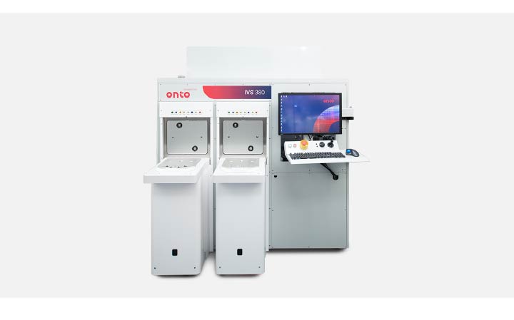
The IVS 380 System performs overlay, CD, and height metrology for 300mm wafers.
The KLA .204 PSL Wafer is an 8-inch NIST-traceable reference wafer compatible with Surfscan 6xy0 and Sp1 particle counters.