SPTS
Synapse
The SPTS Synapse is an ICP-based high-density plasma source etcher. The Synapse is dedicated to the etching of silicon dioxide and silicon nitride layers. The Synapse features a high density plasma source, wafer voltage biasing independent from the ICP, electrostatic clamping, a loadlock/chamber transfer system, and optical emission spectroscopy and laser reflectometry/interferometry end-point detection.[1]
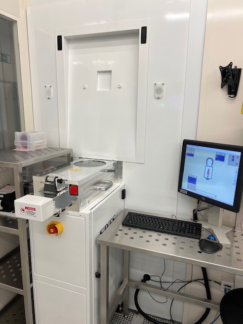
Plate 01(UPDATED!) Unbelievable! SPTS Auto Farm Stats with *NEW Script 2023* - #Roblox #Synapse
HiroWatch on YouTubePlate 02Unbelievable! SPTS Auto Farm Stats with *NEW Pastebin 2023* - #Roblox #Synapse
HiroWatch on YouTubePlate 03how Synapse helps analysts uncover connections that would otherwise be difficult to spot. #cti
The Vertex Project | Synapse Enterprise Watch on YouTubePlate 04Synapse V2 Force Board Edition Takes Prix Du Jury at Reeduca 2026
SynapseWatch on YouTubePlate 05Get the Golden Thesis Manual Here: https://tally.so/r/PdOgdb
Synapse SprintsWatch on YouTubePlate 06From Total Synapse Loss to 100% Repair: Is J147 the Holy Grail?
Salem SavageWatch on YouTube
How it works
The Synapse module features an ICP-based high-density plasma source. Wafer voltage biasing is independent from the ICP power, allowing separate control of ion energy and ion density. The system uses an electrostatic chuck for wafer clamping, eliminating the need for edge-bead removal (EBR). A powerful gas process pumping arrangement is provided, and the tool supports single-wafer processing via a loadlock/chamber transfer system.[1]
Process control includes fully automated software, optical emission spectroscopy (OES) for end-point detection in monitoring-only mode, and laser reflectometry/interferometry for end-point detection. The wafer is cooled by backside helium flow, with continuous monitoring of the helium flow for a preset pressure. The system can run automatic chamber cleaning cycles after each wafer, based on end-point detection.[1]
A typical process sequence involves loading the wafer, clamping it with the electrostatic chuck, applying helium backside cooling, running the etch step with end-point monitoring optionally, then dechucking with a low-power argon plasma to remove accumulated charges, and unloading. If needed, an automatic dry clean of the chamber and chuck follows.[1]
Applications
The system supports multiple mask materials including photoresists (ZEP, CSAR, JSR M108Y, JSR M35G, DUV42P) and can etch with various gas combinations. End-point detection via OES and laser reflectometry is available for process control. The tool also performs automatic dry cleaning using O2 plasma and can be used for extended etches by splitting the process into multiple steps with cleaning in between.[1]
- Etching SiO2 layers
- Etching SixNy layers
- Single-wafer plasma etching
Why won't it start?
Documented failure modes, common issues, and field considerations.
- The etcher must not be exposed to any metallics or traces of metallics.
- Wafers that were once in contact with metallic layers, including buried metallic layers, must not be loaded.
- Wafers previously processed in SPTS APS etcher are not allowed in SPTS Synapse.
What do the numbers mean?
Wafer handling1
Gas & chemistry5
- Gas flow rates
- O2 0-200 sccm; Ar 0-140 sccm; He 0-500 sccm; H2 0-100 sccm; SF6 0-200 sccm; C4F8 0-60 sccm; CF4 0-50 sccm; CHF3 0-100 sccm[1]
- Etch rate (SiO2)
- 320 nm/min (with C4F8/H2/He chemistry and PR mask); 400 nm/min (with C4F8/H2/He chemistry and PR mask, APS_SiO2_PR_3:1 process)[1]
- Etch rate (Si3N4)
- 180 nm/min (with CHF3/SF6/H2 chemistry, smooth process); 190 nm/min (with CHF3/SF6 chemistry, APS_Si3N4_Smooth process)[1]
- Gases available
- O2 [0 – 200 sccm], Ar [0 – 140 sccm], He [0 – 500 sccm], H2 [0 – 100 sccm], SF6 [0 – 200 sccm], C4F8 [0 – 60 sccm], CF4 [0 – 50 sccm], CHF3 [0 – 100 sccm][1]
Optics & imaging5
- Endpoint detection
- Optical Emission Spectroscopy (EOS) and laser reflectometry/interferometry[1]
Configuration & options7
What replaced it?
Related models
- siblingAlcatel AMS 200 SE— Listed in the same etching equipment section.source[2]
What does it need to run?
Site utility requirements, footprint, and infrastructure needed to install and operate this tool. Sourced from public records.
- Gases availableO2, Ar, He, H2, SF6, C4F8, CF4, CHF3[1]
- Gas flow ratesO2 0-200 sccm; Ar 0-140 sccm; He 0-500 sccm; H2 0-100 sccm; SF6 0-200 sccm; C4F8 0-60 sccm; CF4 0-50 sccm; CHF3 0-100 sccm[1]
- Etch rate (SiO2)320 nm/min (with C4F8/H2/He chemistry and PR mask); 400 nm/min (with C4F8/H2/He chemistry and PR mask, APS_SiO2_PR_3:1 process)[1]
- Etch rate (Si3N4)180 nm/min (with CHF3/SF6/H2 chemistry, smooth process); 190 nm/min (with CHF3/SF6 chemistry, APS_Si3N4_Smooth process)[1]
- Gases availableO2 [0 – 200 sccm], Ar [0 – 140 sccm], He [0 – 500 sccm], H2 [0 – 100 sccm], SF6 [0 – 200 sccm], C4F8 [0 – 60 sccm], CF4 [0 – 50 sccm], CHF3 [0 – 100 sccm][1]
Where are the manuals?
Publicly hosted documents referencing this tool, linked at their original location. Hosted by the linked institutions — availability may change.
- Step-by-step usermanualManualepfl.ch
Generated from public-source data on file. Enter your email to access — nothing is published; details are routed privately.
Not publicly documented
Field notes
No research found yet — worked with this tool? Share what you know.
Frequently asked questions
Which materials can be etched on the SPTS Synapse?
The Synapse is dedicated to etching silicon dioxide (SiO2) and silicon nitride (SiNx) layers. Sapphire wafers and ALD-deposited Al2O3 layers are accepted. Wafers that have ever been in contact with metallic layers (even buried) must not be loaded.[1]
What are typical etch rates and selectivities for SiO2 and Si3N4?
For a process named 00_CMi_SiO2_PR using C4F8/H2/He chemistry, the SiO2 etch rate is 320 nm/min with a selectivity to photoresist of 4:1. For 00_CMi_Si3N4_Smooth using CHF3/SF6/H2, the Si3N4 etch rate is 180 nm/min and selectivity to photoresist is >2.5:1. Another Si3N4 process (APS_Si3N4_Smooth) gives 190 nm/min with selectivity >1.5:1.[1]
How is end-point detection performed?
The system provides optical emission spectroscopy (OES) and laser reflectometry/interferometry for end-point detection. The OES system operates in monitoring-only mode and does not control the process chamber; the operator must manually stop etching if end point is detected, otherwise the process runs to the set time.[1]
What are the restrictions regarding metallic contamination?
The Synapse must not be exposed to any metallics or even traces of metallics. Wafers that have ever been in contact with layers of metallics (even buried) or traces of metallics must not be loaded. Wafers previously processed in the SPTS APS etcher are also not allowed in the Synapse.[1]
What is the maximum allowed etch time per step?
The maximum allowed etch time per step is 20 minutes. For longer etches, the process must be split into several steps, allowing an automatic O2 dry clean to proceed between each.[1]
Not publicly documented
The following facts about the Synapse are absent from this record as of this revision. First-hand knowledge or a citation closes a gap; every submission is reviewed before publication.
No publicly documented production dates or lifecycle milestones (introduction, end of production, EOL) for the Synapse are on record.
Answerable by: OEM historical records or a trade-press announcement
No publicly documented variants, configuration options, or revision breakpoints of the Synapse are on record.
Answerable by: an OEM product catalog or an engineer who ordered or specified the tool
The control-system platform and OS era of the Synapse are not on record.
Answerable by: an engineer who operated it or OEM installation records
The process node or technology generation of the Synapse is not on record.
Answerable by: an OEM datasheet or a fab qualification report
No publicly documented compatible parts, consumables, or accessories for the Synapse are on record.
Answerable by: an OEM parts catalog or a service engineer
Sources & citations
Sources (3)Every fact above is drawn from these public sources
- [1]epfl.ch — epfl.chepfl.ch
- [2]epfl.chepfl.ch
- [3]SPTS Etch Process Solutions for LED Manufacturing — spts.com (Feb 28, 2018)web.archive.org
Last updated Oct 8, 2026.
Compare with similar tools
View all →The Applied Materials 0010-47763 is an electrostatic chuck (ESC) assembly used in semiconductor etching processes.
The Applied Materials 0010-16392 is an electrostatic chuck assembly designed for 300 mm wafer processing, featuring a dual electrode configuration.
Oxford Instruments 100 ICP Fluorine is an inductively coupled plasma etcher for fluorine-based etching, supporting cryo DRIE and multiple etch gases including SF6 and C4F8.
