Raith
EBPG5200
The Raith EBPG5200 is an electron beam lithography tool. The Raith EBPG5200 operates at 100 kV. The Raith EBPG5200 has a 125 MHz pattern generator.[1][2]
What it is
General reference — not yet source-verifiedThe Raith EBPG5200 is an electron beam lithography system used for direct-write patterning on electron-sensitive resists.
The EBPG5200 belongs to the dedicated electron beam lithography class and is used for high-resolution pattern generation with beam energy and stage control suited to nanofabrication work.
How it works
Where it fits in the process flow
Applications
The EBPG5200 is used for high-resolution patterning of standard semiconductor materials, low-vapor-pressure metals, and e-beam resists.[1][2]
- High aspect ratio nanostructures
- High speed direct write
- Batch production
- Compound semiconductor devices
- Anticounterfeiting security elements
What do the numbers mean?
Power & electrical4
Wafer handling1
Optics & imaging6
Configuration & options8
Vintage & configurations
Documented models & variants
| Designation | Generation | Vintage | Changes | Source |
|---|---|---|---|---|
| EBPG5200+ | — | — | Described as an electron beam lithography tool capable of high resolution patterning at 100 kV with a 125 MHz pattern generator, 350 nA maximum current, and 1 mm mainfield size. | wiki.nano.upenn.edu[1] |
What does it need to run?
Site utility requirements, footprint, and infrastructure needed to install and operate this tool. Sourced from public records.
Where are the manuals?
Generated from public-source data on file. Enter your email to access — nothing is published; details are routed privately.
Not publicly documented
Field notes
No research found yet — worked with this tool? Share what you know.
Frequently asked questions
Is an electron-beam lithography system maskless?General reference — not yet source-verified
Yes, for direct-write use. The pattern is transferred directly into electron-sensitive resist, so no physical photomask is needed. The same system can also write the masks used by optical lithography.
What types of substrate materials can be patterned?General reference — not yet source-verified
Common substrates include silicon wafers, compound semiconductor wafers, glass or quartz mask blanks, and small experimental coupons. The main practical requirements are that the substrate fit in the vacuum chamber and that its surface dissipate charge or be treated to avoid charging during exposure.
What are the limitations of electron-beam lithography?General reference — not yet source-verified
Because the beam writes features serially, throughput is low compared with optical exposure systems. The exposure is also sensitive to charging, drift, and other beam-placement errors, so careful tool control and calibration are needed to achieve good overlay and resolution.
How is a pattern prepared for exposure?General reference — not yet source-verified
The pattern is first designed in layout software and converted into the exposure data format used by the system. The pattern generator then interprets that data and directs the beam deflection and stage motion to write the layout into the resist layer.
What resists are commonly used?General reference — not yet source-verified
Both positive and negative electron-beam resists are used. Positive resists become more soluble where exposed, leaving the unexposed pattern; negative resists become less soluble where exposed, leaving the exposed pattern after development.
Not publicly documented
The following facts about the EBPG5200 are absent from this record as of this revision. First-hand knowledge or a citation closes a gap; every submission is reviewed before publication.
No publicly documented production dates or lifecycle milestones (introduction, end of production, EOL) for the EBPG5200 are on record.
Answerable by: OEM historical records or a trade-press announcement
The control-system platform and OS era of the EBPG5200 are not on record.
Answerable by: an engineer who operated it or OEM installation records
No publicly documented failure modes or field errata for the EBPG5200 are on record.
Answerable by: a field service engineer, process engineer, or maintenance technician
The process node or technology generation of the EBPG5200 is not on record.
Answerable by: an OEM datasheet or a fab qualification report
No publicly documented compatible parts, consumables, or accessories for the EBPG5200 are on record.
Answerable by: an OEM parts catalog or a service engineer
No research found yet — worked with this tool? Share what you know.
Sources & citations
Sources (6)Every fact above is drawn from these public sources
- [1]wiki.nano.upenn.edu — wiki.nano.upenn.eduwiki.nano.upenn.edu
- [2]Singh Center for Nanotechnology — nano.upenn.edunano.upenn.edu
- [3]web.archive.org — web.archive.orgweb.archive.org
- [4]waferpedia.com — waferpedia.comwaferpedia.com
- [5]nanolabnl.nlnanolabnl.nl
- [6]Raith EBPG5200 plus – Ebeam tool ‒ Center of MicroNanoTechnology CMi ‐ EPFL — epfl.chepfl.ch
Last updated Oct 9, 2026.
Compare with similar tools
View all →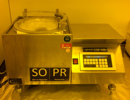
The CEE 100 is a lithography spin coater/developer tool that accepts up to 6-inch wafers and supports programmable multi-step processing.
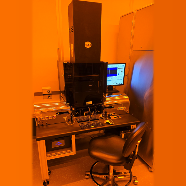
The OAI 806 Mask Aligner is a precision photolithography tool for patterning substrates up to 6 inches with soft, hard, and proximity contact modes.

Heidelberg Instruments DWL66 is a high-resolution direct write pattern generator for direct writing on various substrates and mask making.
